CPO test equipment is chasing a device target that keeps moving
Test vendors are building CPO production tooling while connector standards, laser sources, and optical-engine designs are still in flux - a structural mismatch the industry has not yet resolved.
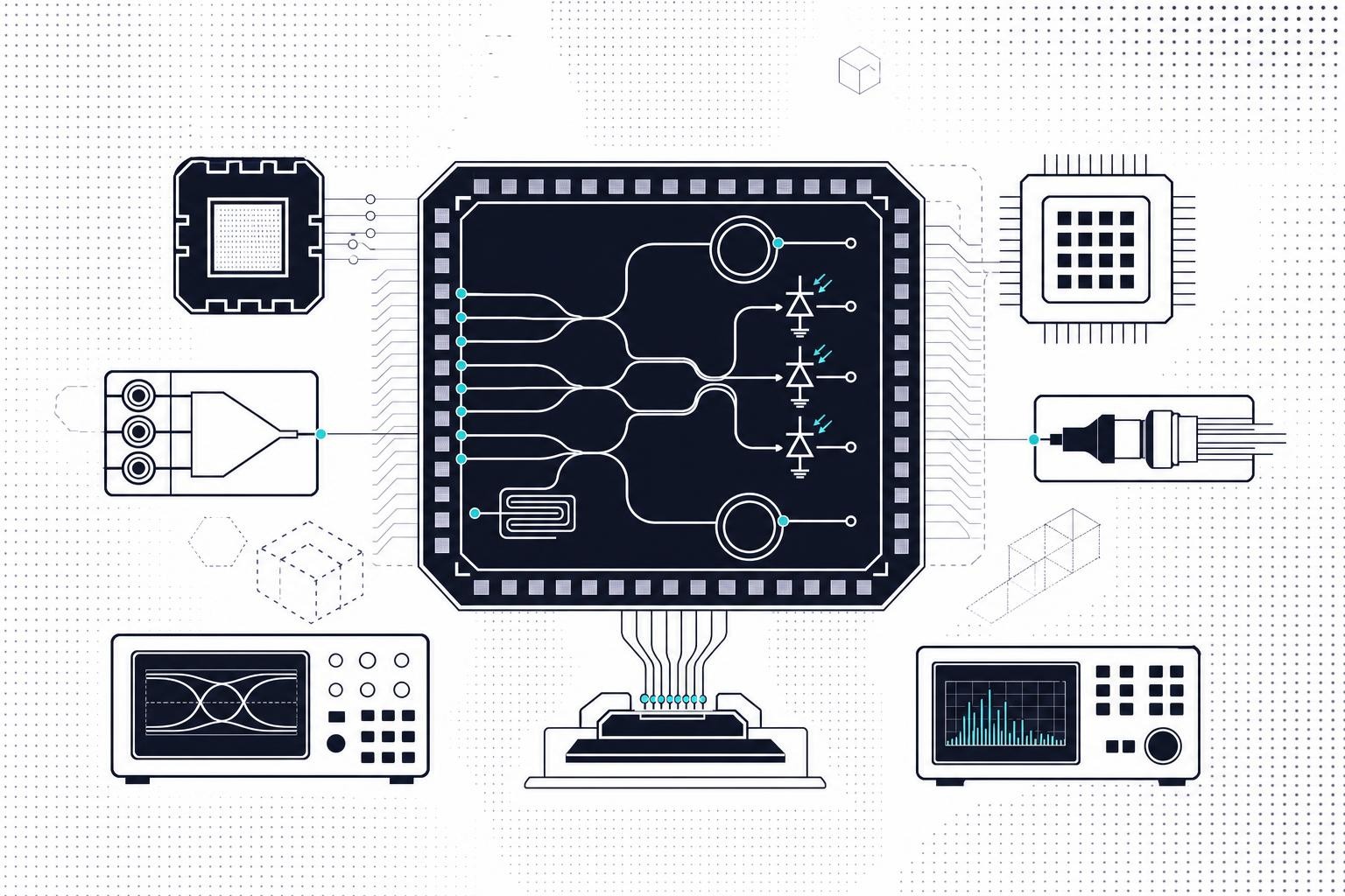
As massive data centers begin deploying the first waves of co-packaged optics (CPO) and near-packaged optics (NPO), test vendors are being asked to deliver high-volume manufacturing tooling for devices whose fundamental specifications - connector types, laser sources, optical-engine counts - are still being decided[1]. The mismatch is not a temporary inconvenience; it is the defining structural problem for CPO test in 2026.
The scan-test gap
The most direct way to frame the problem comes from ISE Labs fellow Dave Armstrong, speaking to Semiconductor Engineering: CPO test today resembles digital logic test before scan was invented[1]. Engineers are reaching for rack-and-stack bench instruments and custom alignment rigs - the same approach that proved "clunky, cumbersome, and slow" in an earlier era of electronics - because design-for-test (DFT) methodology has not yet been developed for optical devices[1]. Without it, every waveguide, resonator, and photodiode must be probed individually, a process that does not scale[1].
The numbers make the bottleneck concrete. 100% inspection of a single photonic IC currently takes on average more than 100 seconds using manual fiber-alignment techniques, according to TrendForce. Scaling CPO to production demands moving from roughly one million units per year today toward tens of millions[1], and manual alignment is simply not viable at that throughput.
Alignment tolerances that dwarf electronics
Optical components impose physical constraints that have no direct equivalent in electrical ATE. Keysight silicon photonics researcher Kazuo Yamaguchi notes that multi-channel optical connectivity shows design variation from unit to unit and channel to channel - a measurement on channel 1 of a waveguide differs from the same measurement on channel 2[1]. Teradyne's Matt Griffin puts the automation challenge plainly: the industry needs to move from characterization-lab fiber alignment to a test floor running many parallel testers, with full software, data-analysis, and test-programming infrastructure behind them[1].
The sensitivity gap versus electronics shows up in three specific areas:
- Thermal and warpage effects - optical coupling is disrupted by package deformation that would be inconsequential for an electrical contact[1].
- Sub-micrometer fiber alignment - electrical probers typically achieve alignment within tens of micrometers; optical probers must hit sub-micrometer precision to avoid signal loss and measurement error.
- Polarization and calibration drift - parameters such as polarization extinction ratio, insertion loss, and responsivity require optical calibration that has no established traceable standard at production scale[1].
No connector standard, no reusable test cell
Current CPO designs integrate anywhere from 4 to 36 optical engines across two to four sides of a compute die, and the industry still lacks a common approach to fiber connectors, alignment schemes, and laser delivery, according to Teradyne's Griffin. The result is that every CPO design requires a bespoke test-cell solution - longer time to market, higher cost, and no equipment reuse across programs. Advantest America vice president Ira Leventhal describes the situation as one where customers are still deciding which connection technologies and laser sources they will use, meaning test vendors are designing tooling for a specification that may change before the product ships[1].
Efforts to break the deadlock are under way. Lightmatter and Open Compute Project partners announced a reference design aimed at enabling the ecosystem to scale toward 10 million units per year, with test specifications included. SENKO, Advantest, and VIAVI demonstrated an integrated automated test platform in September 2026 targeting repeatable high-volume CPO final test at 200 Gb/s per lane through a detachable optical connector.
The pace at which connector and laser-source choices converge will determine whether test vendors can build reusable, cost-effective tooling before the volume ramp arrives - or whether the industry repeats the bespoke-equipment cycle one generation at a time.
Written by Electronics Insider's automated desk from the sources above and published automatically. How we work.
Related
 Design & EDA
Onto Innovation extends FAaST platform to map residual surface charge across wafers and panels in advanced packaging
Onto Innovation published details on 8 October 2026 of how its FAaST non-contact electrical metrology platform addresses residual charge buildup in advanced packaging flows.
13 Oct 2026 Semiconductors
Galileo wins permits for two 125 MW battery storage projects in Italy, totalling 1.5 GWh
Zurich-based developer Galileo has secured planning consent for 250 MW / 1.5 GWh of battery storage in Italy, with a further ~100 MW expected in the coming weeks.
13 Oct 2026 Semiconductors
Pasqal moves Q-PLANET, its €50 million EU neutral-atom chip pilot line, into execution phase
French quantum company Pasqal has transitioned the €50 million Q-PLANET pilot line into active execution, targeting industrial-grade chip components for neutral-atom quantum systems across 11 EU countries.
13 Oct 2026