Lam Research's Semiverse Solutions shows feedforward control lifting wafer pass rates from 61% to 97% in digital twin simulation
Lam Research's Semiverse Solutions used SEMulator3D digital twin simulation to show feedforward etch control raising wafer pass rates from 60.82% to 96.77% and improving Cpk 2.5x.
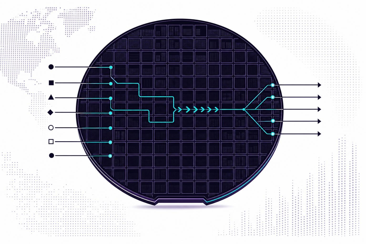
Lam Research's Semiverse Solutions team published a study on 20 August 2026 showing that a feedforward control strategy applied to a lithography-to-etch process sequence can raise wafer pass rates from 60.82% to 96.77% - a gain demonstrated entirely through SEMulator3D digital twin simulation, without committing a single physical wafer[1].
The problem feedforward control is trying to solve
Semiconductor yield is a constant battle against process variability[1]. Every wafer that falls out of specification represents lost time, lost capacity, and lost value[1] - a problem that grows more acute as wafer costs climb. TSMC's 3 nm wafers are priced at roughly $20,000 each in 2026, meaning even a modest improvement in pass rate translates directly into recoverable revenue.
Conventional approaches sit at two extremes. Open-loop fabrication ignores variation entirely and accepts the resulting yield loss. Traditional feedback control reacts only after wafers have already missed specification[1]. Feedforward control takes a different path: it measures each wafer after lithography and adjusts the downstream etch step to compensate for incoming variability before defects occur[1].
How the simulation was structured
The Semiverse Solutions team ran 500 SEMulator3D simulation runs, each representing one wafer, through a lithography-then-etch process sequence[1]. Controlled variability was introduced at the lithography step to replicate the wafer-to-wafer variation that arises when resist spin coating, exposure, and development are not tightly held between runs[1].
The resulting lithography critical dimension (CD) distribution had a mean of 60.12 nm with a standard deviation of 2.06 nm[1]. Even with a tightly controlled etch process, that incoming spread propagated through to a post-etch CD mean of 35.39 nm with a standard deviation of 2.07 nm[1]. Setting specification limits at ±5% of CD, the baseline post-etch Cpk was 0.28 - a figure that indicates a process well outside acceptable capability[1].
The binning strategy and its results
Rather than computing a unique etch recipe for every wafer, the team sorted wafers into three bins based on their post-lithography CD measurement:
- CD below 59 nm (under target): etch isotropy scaled down by 11.7%, reducing CD loss and lifting post-etch CD toward target[1]
- CD between 59 nm and 61 nm (near target): standard etch recipe applied[1]
- CD above 61 nm (over target): etch isotropy adjusted upward to trim excess CD[1]
Routing each wafer to its matched recipe improved post-etch Cpk from 0.2854 to 0.7135 - a 2.5x gain - and pushed the pass rate from 60.82% to 96.77%[1]. The study notes that substantial gains were preserved even as lithography variability increased beyond nominal conditions[1].
Throughput is the trade-off to watch
The study is candid that pass rate alone is the wrong metric. Feedforward control requires recipe-specific etch time changes that can slow wafer throughput[1]. The team's argument is that higher pass rates create headroom to absorb those recipe-related slowdowns and still produce more good wafers per unit time[1] - but that arithmetic depends on the magnitude of the throughput penalty, which will vary by tool and process.
The next test for this approach is calibration against real fab data. SEMulator3D is a physics-driven voxel modeling platform, and the etch isotropy values used here - 0.125 for the hard mask step and 0.055 for the mandrel step - were chosen to represent a tightly controlled process[1]. Fabs with wider etch variation will need to validate whether the three-bin scheme captures enough of their CD distribution to deliver comparable yield gains, or whether a finer binning strategy is warranted.
Written by Electronics Insider's automated desk from the sources above and published automatically. How we work.
Related
 Semiconductors
Token spend is becoming a line item in EDA project budgets, DAC roundtable finds
A closed-door DAC 2026 roundtable with Cadence, Synopsys, Siemens EDA, Keysight, and ChipAgents found token cost has moved from an afterthought to a formal budget concern in chip design projects.
10 Sept 2026 Design & EDA
Cadence's Amol Borkar explains why AI voice at the edge demands a rethink of SoC architecture, not just faster processors
Semiconductor Engineering's interview with Cadence's Tensilica DSP lead lays out why NLP is reshaping audio SoC design - and why raw clock speed is the wrong lever to pull.
10 Sept 2026 Design & EDA
French gendarmerie researchers show voltage glitching bypasses eMMC password locks on 3 of 10 commercial parts, with measurable evidence alteration
A paper from France's Institut de Recherche Criminelle quantifies both the success rate and the data-integrity cost of fault-assisted eMMC access in forensic investigations.
10 Sept 2026