Imec finds contact formation caps 2D GAA CFET pitch at 36 nm for the A2 node
Imec's July 2026 arXiv paper shows 2D GAA CFETs offer no contacted poly pitch advantage over silicon at A2, with contact resistance and parasitic capacitance as the binding constraints.
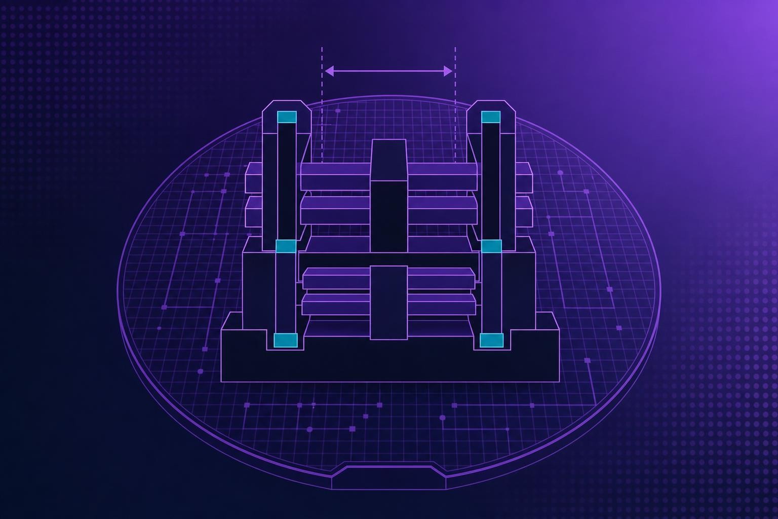
Researchers at imec published a paper on 14 July 2026 concluding that gate-all-around complementary field-effect transistors built on atomically thin two-dimensional semiconductors do not deliver the pitch scaling benefit that had been widely anticipated for the A2 logic node[1]. The key number: contact formation constraints impose a minimum contacted poly pitch (CPP) of 36 nm for 2D GAA CFETs - identical to the floor already set by silicon GAA CFETs[1].
What the paper examined
The imec team, led by Fengben Xi and 17 co-authors, developed an A2-oriented 2D CFET integration flow targeting a CPP of 36 nm and a gate length (Lg) of 10 nm, and demonstrated several key process modules[1]. To evaluate the architecture rigorously, they built a multiscale power-performance-area (PPA) framework that spans:
- Quantum transport simulations
- Compact-model generation
- A2-targeted GAA integration-flow definition
- Parasitic extraction
- Circuit-level benchmarking[1]
The channel materials under study are transition-metal dichalcogenides (TMDs) - semiconductors such as MoS₂, WS₂, and WSe₂ that can be deposited in layers only a few atoms thick. Their atomically thin body is attractive because it suppresses short-channel effects at gate lengths below 10 nm, where conventional silicon channels begin to lose electrostatic control.
Where the expected gains evaporate
The analysis found that two non-idealities dominate device behavior and erode the theoretical PPA advantage:
- High contact resistance. The interface between a three-dimensional metal contact and an atomically thin 2D channel creates current-crowding effects that drive up resistance, a problem the field has tracked for years but has not yet solved at production-relevant pitches.
- Layout-induced parasitic capacitances. At A2 ground rules, parasitic capacitances arising from the cell layout become the dominant capacitive load, not the intrinsic gate capacitance.
Architectural optimization can improve the effective current-to-capacitance ratio (Ieff/Ceff), but the associated rise in absolute capacitance limits circuit-level gains[1]. In other words, tuning the device geometry to push one metric tends to worsen another, leaving net circuit performance below what the intrinsic channel properties would suggest.
The paper's conclusion is direct: meaningful progress will require co-optimization of contacts, transport, and parasitics, together with 2D-specific CFET architectures[1].
Context in imec's broader roadmap
Imec's logic roadmap places CFET introduction in manufacturing at the A7 node, with silicon-channel devices as the baseline[1]. The 2D-channel variant is positioned as a potential route to extend scaling further - but the July paper makes clear that the path is not straightforward. A separate June 2026 result from imec, ASML, and TSMC demonstrated scaled MoS₂ nFETs and WSe₂ pFETs with a 50 nm CPP on 300 mm wafers, described as a step toward fab readiness - but that CPP is still wider than the 36 nm A2 target, underscoring how much contact engineering remains to be done.
The imec paper sets a concrete benchmark for what the field must achieve: contact resistance and parasitic capacitance co-optimization that is specific to 2D CFET geometries, not borrowed from silicon integration flows. Progress on those two fronts - and whether 2D-specific cell architectures can be defined that avoid the layout parasitics seen here - will determine whether 2D GAA CFETs become a viable option at A2 or remain a post-A2 candidate.
Written by Electronics Insider's automated desk from the sources above and published automatically. How we work.
Related
 Semiconductors
Token spend is becoming a line item in EDA project budgets, DAC roundtable finds
A closed-door DAC 2026 roundtable with Cadence, Synopsys, Siemens EDA, Keysight, and ChipAgents found token cost has moved from an afterthought to a formal budget concern in chip design projects.
10 Sept 2026 Design & EDA
Cadence's Amol Borkar explains why AI voice at the edge demands a rethink of SoC architecture, not just faster processors
Semiconductor Engineering's interview with Cadence's Tensilica DSP lead lays out why NLP is reshaping audio SoC design - and why raw clock speed is the wrong lever to pull.
10 Sept 2026 Design & EDA
French gendarmerie researchers show voltage glitching bypasses eMMC password locks on 3 of 10 commercial parts, with measurable evidence alteration
A paper from France's Institut de Recherche Criminelle quantifies both the success rate and the data-integrity cost of fault-assisted eMMC access in forensic investigations.
10 Sept 2026