AI is compressing the design cycle - and exposing physical realization as the next bottleneck
As agentic AI shrinks the path to tape-out, the constraint in semiconductor development is migrating downstream - into packaging, multi-physics signoff, and physical realization.
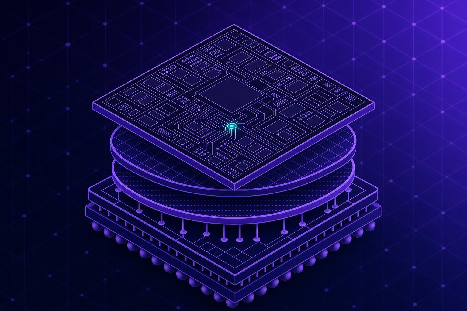
Something consequential is shifting in semiconductor development: the design cycle itself is becoming compressible[1]. The clearest proof point arrived in June 2026, when OpenAI and Broadcom disclosed that their Jalapeño inference ASIC went from initial RTL to tape-out in nine months - a timeline OpenAI described as what may be the fastest ASIC development cycle ever achieved in high-performance advanced semiconductors. Initial RTL work began in February 2025, the design taped out in November, and first silicon arrived in May 2026.
The speed was not accidental. OpenAI used its own models to accelerate parts of the design and optimization process, and Broadcom supplied silicon implementation expertise alongside a close hardware-software co-development model. More than half of the compute die's core was written using the XLS hardware language and compiler infrastructure. The result is a working proof that AI-assisted engineering can meaningfully compress architecture exploration, RTL development, verification, and physical implementation together[1].
The front end is no longer the long pole
EDA vendors have been racing to extend that compression across the full flow. At Synopsys Converge in March 2026, Synopsys unveiled AgentEngineer, which it describes as the industry's first Level 4 orchestrated, multi-agent design and verification workflow. Early customers reported 2× productivity gains, with improvements as high as 5× in select cases. At DAC 2026 in July, Synopsys extended AgentEngineer with autonomous debug closure workflows developed with Microsoft, claiming 25-40% reductions in debug cycle time. Cadence introduced its AuraStack AI Super Agent for PCB and advanced packaging, citing up to 20× faster multiphysics performance. Siemens expanded its Fuse EDA AI Agent system, claiming more than 10× faster library characterization.
The pattern is consistent: front-end tasks that once consumed months are being compressed by agents. That is exactly the dynamic that shifts the constraint elsewhere.
Where the bottleneck lands
When design-to-tape-out cycles shrink, activities that once consumed a smaller fraction of total program time become proportionally larger[1]. The physical realization layer - packaging, multi-physics co-simulation, thermal and mechanical signoff, and known-good-die qualification - does not compress at the same rate as RTL or verification.
The pressure points are well documented:
- Multi-physics co-simulation across 2.5D and 3D stacks has emerged as the binding constraint for chiplet programmes, with computational cost scaling poorly as integration complexity grows.
- Advanced packaging signoff requires co-optimization of electrical, thermal, and mechanical domains under tight power, performance, and area constraints - and conventional high-fidelity solvers make iterative design-space exploration impractical.
- Known-good-die qualification and interposer verification must now be treated as distinct, non-interchangeable steps, adding cost and cycle time that agentic front-end tools do not yet reach.
Intel's Lalitha Immaneni put the problem plainly at DAC 2026: design teams are still too often "jumping blindly" into complex stacks without adequate multi-physics guidance or standardized data, and poor copper-density data can force a foundry's mechanical team to spend three to four weeks cleaning up a database before analysis can begin.
Tools targeting the gap
Vendors are beginning to address the physical layer directly. Synopsys's Multiphysics Fusion portfolio, built on the Ansys acquisition, integrates signoff-grade thermal, electromagnetic, and voltage-drop analysis into the implementation flow. Xpeedic's EDA2026 platform, shown at DAC, adds two-way electro-thermal feedback modeling to its board-level Notus tool, so current and temperature fields solve together automatically rather than through manual handoffs. Startups such as Vinci are training physics foundation models to replace weeks-long thermal and thermomechanical simulations with automated analysis.
The trajectory is clear: as agentic AI continues to compress the front end, the industry's attention - and its next wave of tooling investment - will follow the bottleneck downstream into the physical stack[1]. How quickly multi-physics simulation and advanced packaging signoff can be made as fluid as RTL generation will determine whether the nine-month tape-out becomes a repeatable baseline or remains an outlier.
Written by Electronics Insider's automated desk from the sources above and published automatically. How we work.
Related
 Design & EDA
ETH Zürich and NYU show JEDEC test loops miss worst-case HBM2 power by 23.6%
Researchers at ETH Zürich and NYU tested 36 real HBM2 chips and found JEDEC measurement loops understate peak power by 23.6%, with read ops and data-bus toggling as the main drivers.
15 Oct 2026 Design & EDA
FlowAccel's Joel Jorgensen argues chip teams must design their workflows before AI can help them hit tape-out
Joel Jorgensen of FlowAccel argues that AI tools alone won't save a tape-out schedule - teams must first design the cross-team workflows that let those tools compound into real gains.
15 Oct 2026 Semiconductors
ETH Zürich and NYU find JEDEC test loops underestimate HBM2 power by up to 35.4%
Researchers at ETH Zürich and NYU tested 36 real HBM2 chips and found JEDEC-specified current loops can underestimate peak power by up to 35.4%, with implications for AI accelerator thermal design.
15 Oct 2026