Imec publishes lubrication-elasticity model for predicting bond front velocity in wafer and die bonding
Imec researcher Utkarsh Jain published a lubrication-elasticity model in May 2026 that derives a self-consistent formulation for bond front velocity in flexible-substrate bonding, targeting process control in 3D IC packaging.
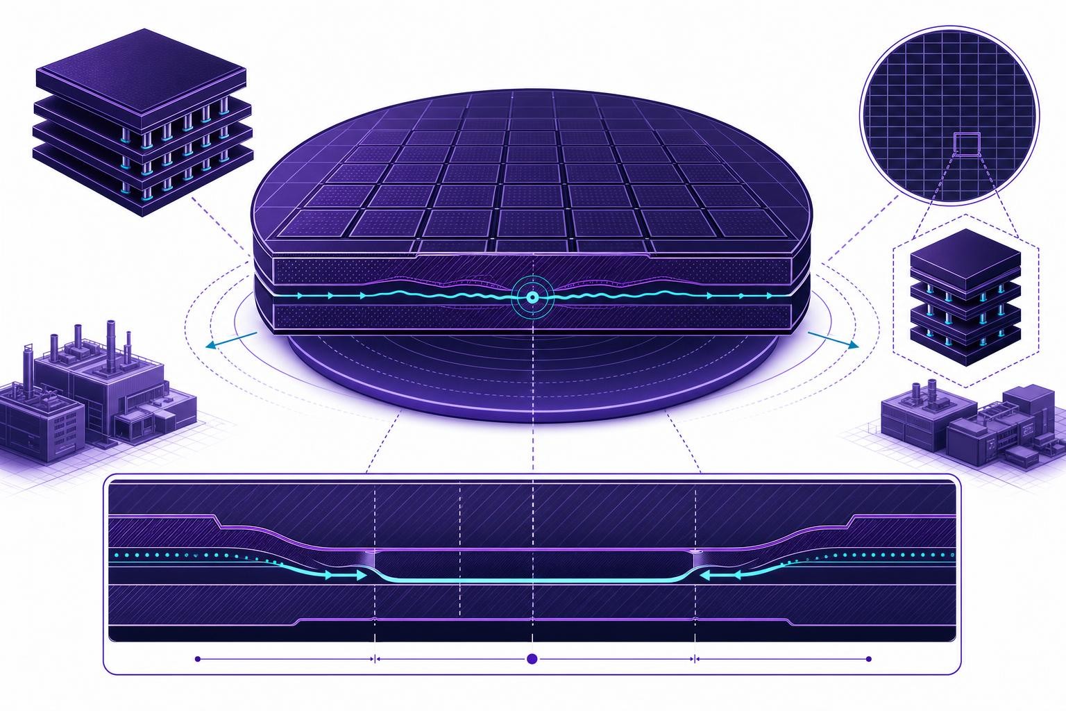
Imec researcher Utkarsh Jain published a paper in the Proceedings of the Royal Society A on 1 May 2026 that derives a self-consistent analytical formulation for bond front velocity during lubrication-mediated bonding of flexible substrates[1]. The work targets process control in wafer and die bonding - assembly steps that have become central to 3D stacking and heterogeneous integration for advanced interconnect architectures[1].
Why bond front velocity matters
When two substrates are brought together, a bond front propagates outward from the point of first contact. The progression of that front is governed by a balance between adhesion and viscous dissipation forces[1]. Getting that balance wrong produces voids - unbonded regions that degrade yield and long-term reliability. Current bonding technology continues to face challenges with unbonded areas, requiring additional annealing to reduce these voids. Void formation before and after annealing presents a critical reliability challenge, as voids can result from trapped gases, surface contamination, or insufficient bonding strength, impacting yield and long-term device performance. A predictive model for front velocity would let process engineers tune parameters before committing wafers to a run.
What the model does
Jain's approach couples lubrication flow in the narrow gap between substrates with linear elasticity in the substrates themselves[1]. The key findings are:
- When governed by lubrication flow and linear elasticity, the unbonded region assumes a power-law shape as a function of distance from the bond front[1].
- The formulation re-parameterizes the problem in terms of a "high viscous dissipation region" that travels ahead of and alongside the adhesion front[1].
- This re-parameterization allows the model to capture bond front acceleration as the unbonded region shrinks - for example, as the front approaches the edge of a finite substrate[1].
- Unifying velocity and length scales are proposed that incorporate a lateral adhesion front length scale, bridging continuum and molecular regimes[1].
The model stays within continuum limits and deliberately excludes adhesion mechanisms, keeping it tractable while still capturing the dominant near-field dynamics[1].
Scope and limitations
The paper is analytical rather than a full finite-element simulation. A separate line of work has developed reduced-order models for wafer-to-wafer bonding by coupling a Kirchhoff-Love plate description of wafer bending to a Reynolds lubrication model, noting that wafer deformation and the entrapped air film interact through a strongly coupled, time-dependent fluid-structure interaction that can produce non-intuitive bonding dynamics. Jain's formulation complements such numerical approaches by offering closed-form scaling laws - substrate thickness, Young's modulus, gas viscosity, and surface energy all feed into the velocity prediction - which are more directly usable for process window definition[1].
The framework is described as scalable, meaning it is intended to apply across both wafer-scale and die-scale bonding geometries[1]. Whether it holds for the thinner, more compliant substrates used in chiplet-on-wafer or panel-level packaging remains an open question the paper does not fully resolve.
The paper is published open-access under a Creative Commons licence[1]. As hybrid bonding pitch continues to shrink and substrate flexibility increases with thinner die, analytical models that connect fluid mechanics to bonding dynamics will be worth watching for adoption in process simulation toolchains.
Written by Electronics Insider's automated desk from the sources above and published automatically. How we work.
Related
 Semiconductors
Token spend is becoming a line item in EDA project budgets, DAC roundtable finds
A closed-door DAC 2026 roundtable with Cadence, Synopsys, Siemens EDA, Keysight, and ChipAgents found token cost has moved from an afterthought to a formal budget concern in chip design projects.
10 Sept 2026 Design & EDA
Cadence's Amol Borkar explains why AI voice at the edge demands a rethink of SoC architecture, not just faster processors
Semiconductor Engineering's interview with Cadence's Tensilica DSP lead lays out why NLP is reshaping audio SoC design - and why raw clock speed is the wrong lever to pull.
10 Sept 2026 Design & EDA
French gendarmerie researchers show voltage glitching bypasses eMMC password locks on 3 of 10 commercial parts, with measurable evidence alteration
A paper from France's Institut de Recherche Criminelle quantifies both the success rate and the data-integrity cost of fault-assisted eMMC access in forensic investigations.
10 Sept 2026