Onto Innovation engineers demonstrate picosecond ultrasonics as an in-line SiCr thickness and excursion monitor for BCD manufacturing
Onto Innovation engineers show how PULSE technology measures SiCr thin-film thickness and detects gas-flow excursions in BCD devices - without touching the wafer.
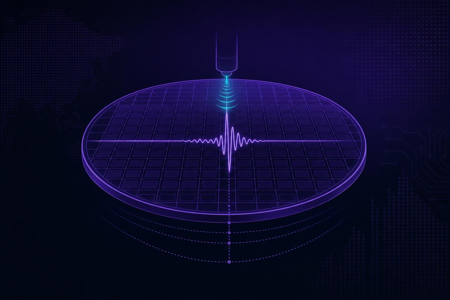
A team of five engineers at Onto Innovation has published a two-part study on Semiconductor Engineering showing that picosecond ultrasonic (PULSE) technology can serve as both a deposition-qualification tool and a real-time excursion monitor for silicon-chromium thin films in bipolar-CMOS-DMOS (BCD) devices[1].
Why SiCr control matters in BCD
BCD devices integrate three complementary transistor types - bipolar, CMOS, and DMOS - onto a single chip, enabling simultaneous handling of analog, digital, and power functions[1]. The architecture is central to automotive, consumer, and medical platforms: automotive systems must manage power, control signals, and safety-critical functions such as braking and airbag deployment, while medical platforms require both precision and reliability[1].
SiCr thin films are the precision resistive elements inside these devices. SiCr resistors offer high stability, low temperature coefficient of resistance (TCR), and excellent linearity, making them well-suited for accurate voltage and current control[1]. The problem is sensitivity: even minor thickness or compositional variations can cause resistance drift, which degrades analog accuracy and long-term reliability[1]. During sputtering, specialty gas-flow variations alter film stoichiometry and microstructure, shifting TCR behavior - including the onset of a pronounced negative coefficient - in ways that are difficult to catch without high-sensitivity in-line monitoring[1].
How PULSE technology works
PULSE technology fires a 0.1 ps laser pulse focused to an approximately 8 × 10 mm² spot onto the wafer surface, generating a sharp acoustic wave[1]. The wave travels through the film at the speed of sound; at each material interface, a portion reflects back to the surface while the rest transmits[1]. A second probe laser detects the returning echoes, and the round-trip transit time is used to calculate film thickness. The technique is non-contact and non-destructive, and it simultaneously captures surface reflectivity data alongside the thickness measurement[1].
That dual-channel output is the key to the second application the team describes. Reflectivity data serves as a qualitative indicator of film morphology and surface roughness - information that thickness alone cannot provide[1]. The engineers show that wafer-level reflectivity variation is substantially larger than thickness variation for films sputtered at different gas-flow rates, making reflectivity the more sensitive signal for catching process excursions before they propagate to downstream electrical test[1].
Two applications from one measurement pass
The study frames PULSE technology's role in two distinct stages of BCD manufacturing:
- Deposition qualification: thickness maps across multiple wafers demonstrate cross-wafer uniformity and lot-to-lot repeatability, the two metrics most critical for qualifying a new SiCr sputtering process[1].
- Excursion monitoring: simultaneously collected reflectivity data flags gas-flow deviations that shift film morphology without producing a detectable thickness change, catching process drift earlier than thickness-only metrology can[1].
The combination means a single in-line measurement step covers both the dimensional and morphological dimensions of SiCr process control - without adding a separate inspection pass or contacting the wafer surface.
Part two of the series, which will address excursion monitoring in greater depth, is forthcoming. The practical question for BCD fabs is whether reflectivity-based monitoring can be tightened into a quantitative control limit, and whether the same platform can be extended to other specialty thin films - such as nichrome or tantalum nitride - that face similar TCR-stability requirements in analog and power management circuits.
Written by Electronics Insider's automated desk from the sources above and published automatically. How we work.
Related
 Semiconductors
Token spend is becoming a line item in EDA project budgets, DAC roundtable finds
A closed-door DAC 2026 roundtable with Cadence, Synopsys, Siemens EDA, Keysight, and ChipAgents found token cost has moved from an afterthought to a formal budget concern in chip design projects.
10 Sept 2026 Design & EDA
Cadence's Amol Borkar explains why AI voice at the edge demands a rethink of SoC architecture, not just faster processors
Semiconductor Engineering's interview with Cadence's Tensilica DSP lead lays out why NLP is reshaping audio SoC design - and why raw clock speed is the wrong lever to pull.
10 Sept 2026 Design & EDA
French gendarmerie researchers show voltage glitching bypasses eMMC password locks on 3 of 10 commercial parts, with measurable evidence alteration
A paper from France's Institut de Recherche Criminelle quantifies both the success rate and the data-integrity cost of fault-assisted eMMC access in forensic investigations.
10 Sept 2026