SemiWiki argues that thermal reliability models miss the mechanical damage temperature inflicts on advanced packages
Temperature does more than age chips - it physically moves them. A SemiWiki analysis explains why Arrhenius-based reliability models fall short for 3D IC and advanced packaging designs.
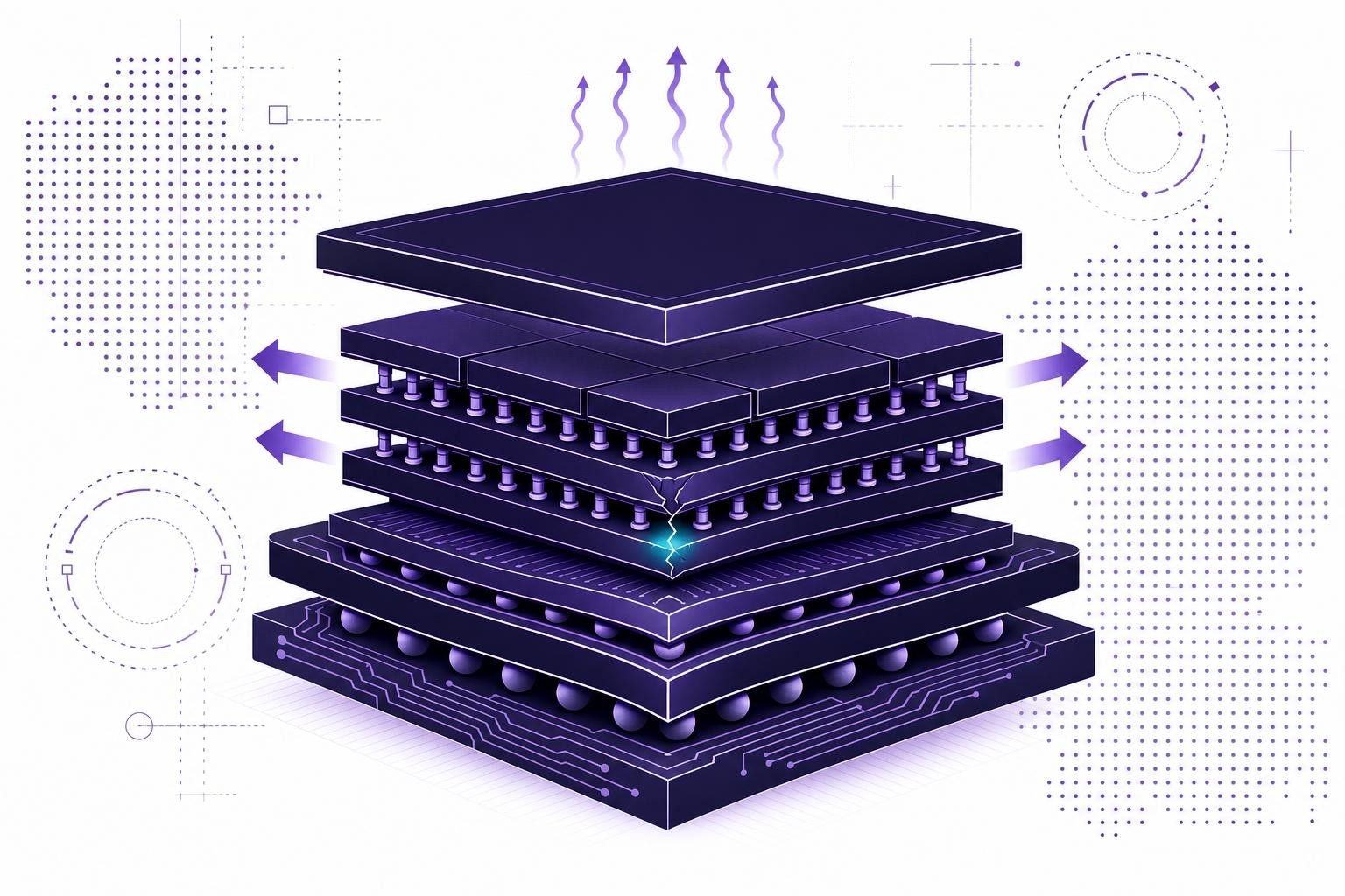
A SemiWiki analysis published in August 2026 makes a pointed argument that the semiconductor industry's standard approach to thermal reliability - treating temperature as a clock that accelerates aging - systematically ignores a second, equally damaging role: temperature physically displaces the materials inside a package[1].
The distinction matters more than it might appear. As 3D IC and chiplet-based designs push dissimilar materials into ever-closer contact, the mechanical consequences of heat have become a primary yield and reliability driver in their own right.
The Arrhenius assumption and where it breaks down
The dominant framework for thermal reliability is the Arrhenius acceleration model. The model is used in accelerated life testing and assumes that the failure mechanism follows a thermally activated process, meaning that increasing temperature exponentially accelerates the failure rate. That works well when a single, well-characterised chemical mechanism - diffusion, oxidation, an interfacial reaction - dominates the failure population.
The problem is that real packages rarely present a single mechanism. Use of the Arrhenius equation for burn-in and life-test data has been called into question because the validity of the Arrhenius activation energy is asserted to be restricted to only one failure mechanism; if multiple failure mechanisms apply to an integrated circuit type, the temperature acceleration factor must be complex. The SemiWiki piece makes the same point: the approach is only valid when the dominant failure mechanism is known, its thermal activation behaviour is understood, and that same mechanism remains active throughout the test[1].
The Arrhenius model applies primarily to thermally activated failure mechanisms such as chemical degradation, diffusion, or interfacial reactions; for failures driven by mechanical, electrical, or multi-factor stresses, the model alone may not be sufficient.
How temperature moves a package
The mechanical effect the SemiWiki analysis highlights is coefficient of thermal expansion (CTE) mismatch. Every material in a package expands and contracts at a different rate as temperature changes. On a 3D IC, stress is mainly caused by the incompatible CTE mismatch between materials, which causes warpage and displacement - silicon has a CTE of 2.6 ppm/°C, while typical package substrates sit around 6 ppm/°C and FR4 PCB material reaches 17 ppm/°C.
The failure modes that follow are structural, not chemical:
- Dielectric cracking, interfacial delamination, solder joint fatigue, and copper trace fracture are all package-level failure modes driven by thermo-mechanical stress[1]
- In 3D stacks, stresses concentrate in micro-bump arrays, hybrid bonding interfaces, TSV regions, and underfill layers; even when average die temperatures remain within specification, spatial gradients and transient swings - especially under bursty AI workloads - can accelerate fatigue mechanisms including interconnect cracking and interface degradation
- The stress generated during temperature cycling can cause chip metallisation to move or deform
Warpage control has become a defining challenge as panel-level packaging scales toward advanced AI chip packaging, with CTE mismatch between materials compounding in ways that directly affect yield. As panel size grows and layer counts increase, thermal stress from CTE mismatches between materials compounds in ways that directly affect yield.
What this means for design and verification
The implication for EDA flows is that thermal analysis cannot be confined to a reliability sign-off step that asks only "how fast does this age?" It must also answer "how far does this move, and what breaks when it does?"
In a temperature-aware timing analysis flow, parasitic extraction and delay calculation are done in two passes: a first pass calculates parasitics and delays at the average temperature condition of the chip, and a second pass scales interconnect resistance and cell delays based on thermal gradients. That handles the electrical side. The mechanical side - warpage, delamination risk, solder joint fatigue life - demands a separate co-simulation discipline that most teams still treat as a packaging afterthought.
In traditional flows, thermal verification is often performed late and driven by simplified models or abstracted boundary assumptions; in dense 3D IC architectures, this approach underrepresents inter-die thermal coupling, interface resistance variability, and material anisotropy.
The SemiWiki argument is ultimately a call for design teams to treat temperature as a mechanical load, not just a chemical accelerant[1]. Whether EDA vendors respond with tighter co-simulation between thermal, stress, and timing engines - or whether the gap persists into the next packaging generation - is the question worth watching.
Written by Electronics Insider's automated desk from the sources above and published automatically. How we work.
Related
 Semiconductors
Token spend is becoming a line item in EDA project budgets, DAC roundtable finds
A closed-door DAC 2026 roundtable with Cadence, Synopsys, Siemens EDA, Keysight, and ChipAgents found token cost has moved from an afterthought to a formal budget concern in chip design projects.
10 Sept 2026 Design & EDA
Cadence's Amol Borkar explains why AI voice at the edge demands a rethink of SoC architecture, not just faster processors
Semiconductor Engineering's interview with Cadence's Tensilica DSP lead lays out why NLP is reshaping audio SoC design - and why raw clock speed is the wrong lever to pull.
10 Sept 2026 Design & EDA
French gendarmerie researchers show voltage glitching bypasses eMMC password locks on 3 of 10 commercial parts, with measurable evidence alteration
A paper from France's Institut de Recherche Criminelle quantifies both the success rate and the data-integrity cost of fault-assisted eMMC access in forensic investigations.
10 Sept 2026