The Silicon Brief - 10 September 2026
Today: Samsung commits to High NA EUV DRAM by 2028 as TSMC, Intel, and ASML form a 12-inch photomask consortium; Kioxia rules out SK Hynix tie-up; Intel locks in fab spending; and South Korea's chip hub gets its funding anchor.
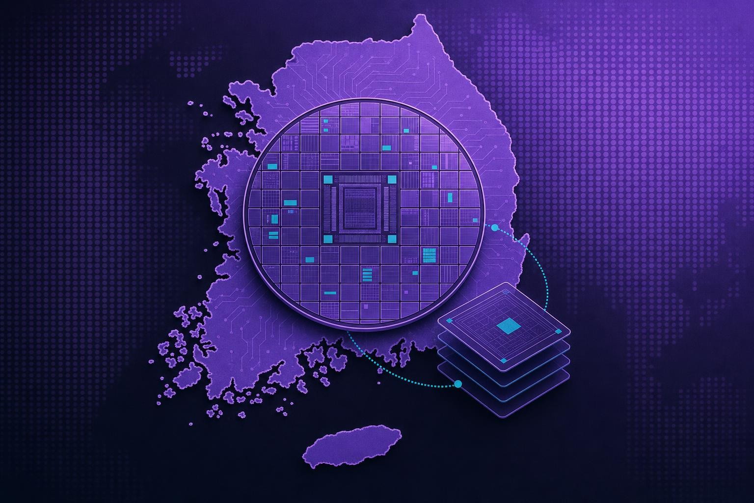
Today's edition covers the semiconductor industry's biggest lithography realignment in decades, a sharp rebuttal from Kioxia's CEO on NAND consolidation, Intel's capital commitment to its European and US fabs, and South Korea's government-backed memory cluster taking shape.
Samsung and ASML announced on 8 September 2026 that Samsung will be the first chipmaker to deploy High NA EUV lithography in DRAM high-volume manufacturing, targeting 2028 - and simultaneously joined TSMC and Intel in a new industry consortium to transition from the 6-inch photomask standard, in use since the 1980s, to a 12-inch format[1]. The 12-inch photomask initiative, announced at the SPIE BACUS Photomask Technology conference in Monterey, targets a pilot line by 2031 and full High NA lithography system readiness for advanced-node production by 2033, with the larger mask area expected to eliminate the roughly 30% stitching throughput penalty that currently limits large-die AI accelerator output. For memory engineers, the 2028 DRAM commitment is the more immediate signal: High NA EUV raises the numerical aperture of projection optics from 0.33 to 0.55, enabling finer features that should extend the DRAM scaling roadmap and simplify process steps[1].
Kioxia Holdings CEO Mutsumi Ota on 9 September 2026 publicly ruled out a manufacturing tie-up with SK Hynix, pushing back on comments made by SK Group chairman Chey Tae-won, who had floated joint NAND production as a way to share the capital burden of AI-driven capacity expansion. Ota also pledged to keep memory prices from rising to levels that could suppress long-term AI demand - a notable commitment at a moment when Kioxia and SanDisk together plan more than ¥ 5 trillion in spending to expand their jointly owned facilities in Japan. The rebuff matters because it leaves the NAND market's consolidation question open: SK Hynix must now fund its own expansion, including a 54 trillion won domestic capacity build and a new advanced packaging facility in Indiana.
Intel CFO David Zinsner confirmed on 3 September 2026 that the company's $23 billion August equity raise was pre-funding for committed fab capacity in Ireland, Arizona, and Oregon, not a distress signal, with the spending tied to equipping those sites before the 14A node reaches high-volume manufacturing in 2028. The disclosure, made at Deutsche Bank's 2026 Technology Conference, also put Intel's advanced packaging business on record as a growth driver, with gross margin now described as "comfortably in the 40s" - a figure that will be watched closely by foundry customers evaluating EMIB-T as an alternative to TSMC's CoWoS.
Samsung Electronics and SK Hynix are anchoring a new South Korean semiconductor cluster with a combined 800 trillion won investment plan aimed at expanding memory production capacity for AI infrastructure. The cluster, backed by government land, power, and infrastructure commitments, signals that both companies intend to absorb the capital demands of the current HBM and DRAM cycle domestically rather than through cross-border manufacturing partnerships - a direct counterpoint to the Kioxia-SK Hynix consolidation discussion that Ota closed down on 9 September.
Written by Electronics Insider's automated desk from the sources above and published automatically. How we work.
Related
 Design & EDA
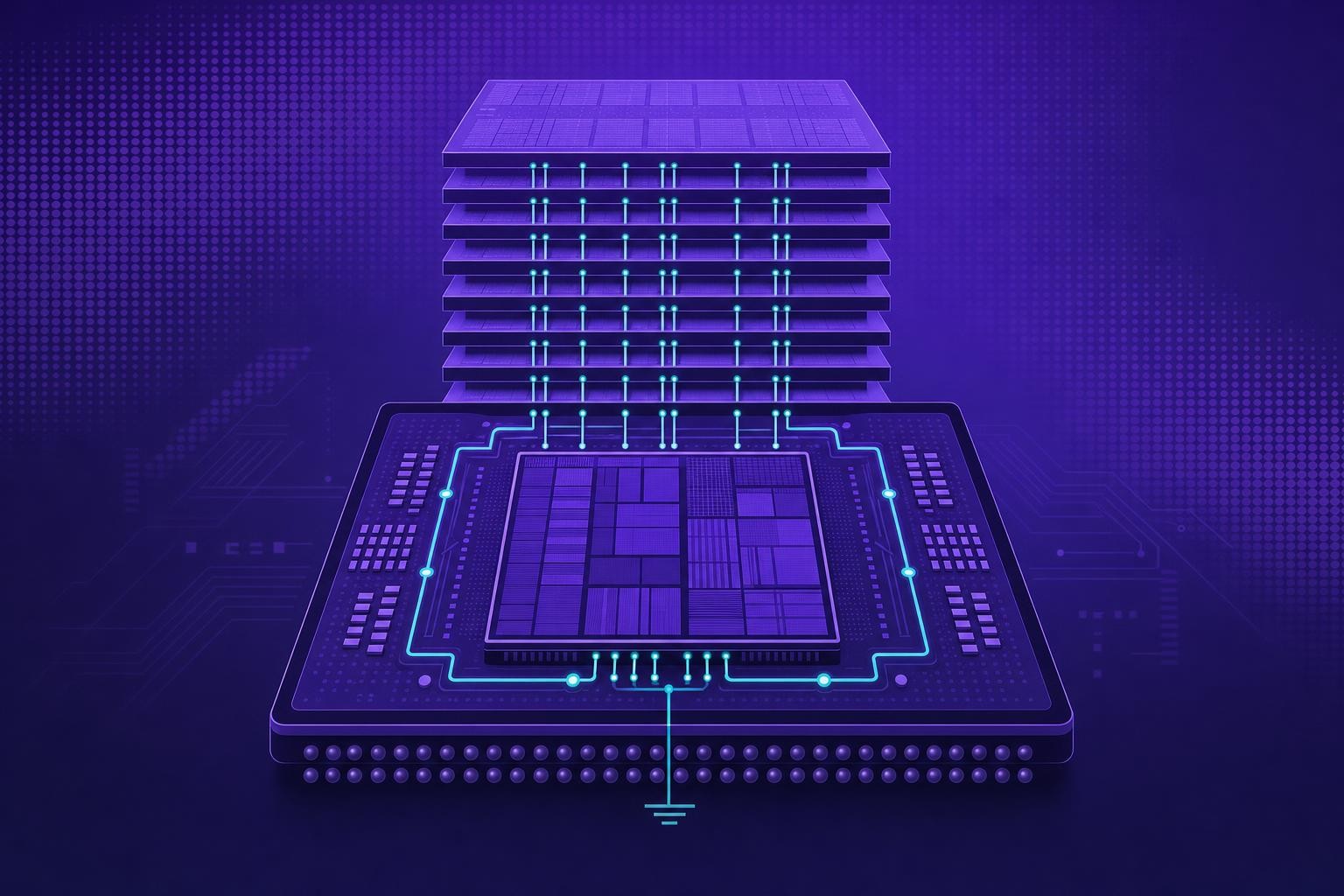
ETH Zürich and NYU show JEDEC test loops miss worst-case HBM2 power by 23.6%
Researchers at ETH Zürich and NYU tested 36 real HBM2 chips and found JEDEC measurement loops understate peak power by 23.6%, with read ops and data-bus toggling as the main drivers.
15 Oct 2026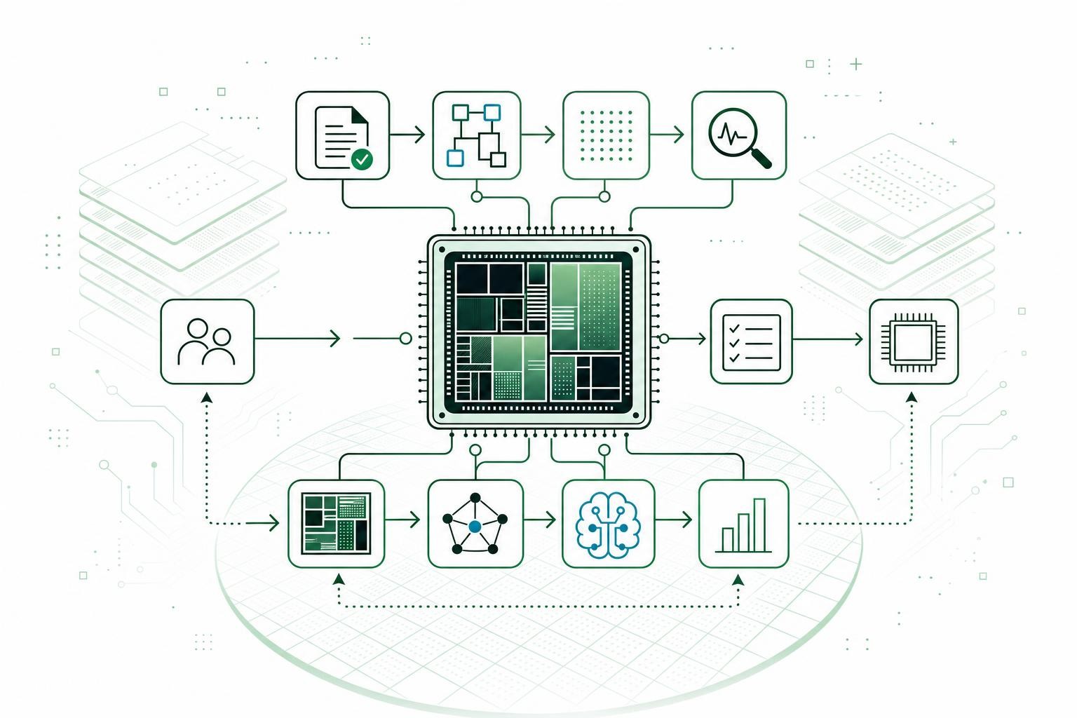 Design & EDA
FlowAccel's Joel Jorgensen argues chip teams must design their workflows before AI can help them hit tape-out
Joel Jorgensen of FlowAccel argues that AI tools alone won't save a tape-out schedule - teams must first design the cross-team workflows that let those tools compound into real gains.
15 Oct 2026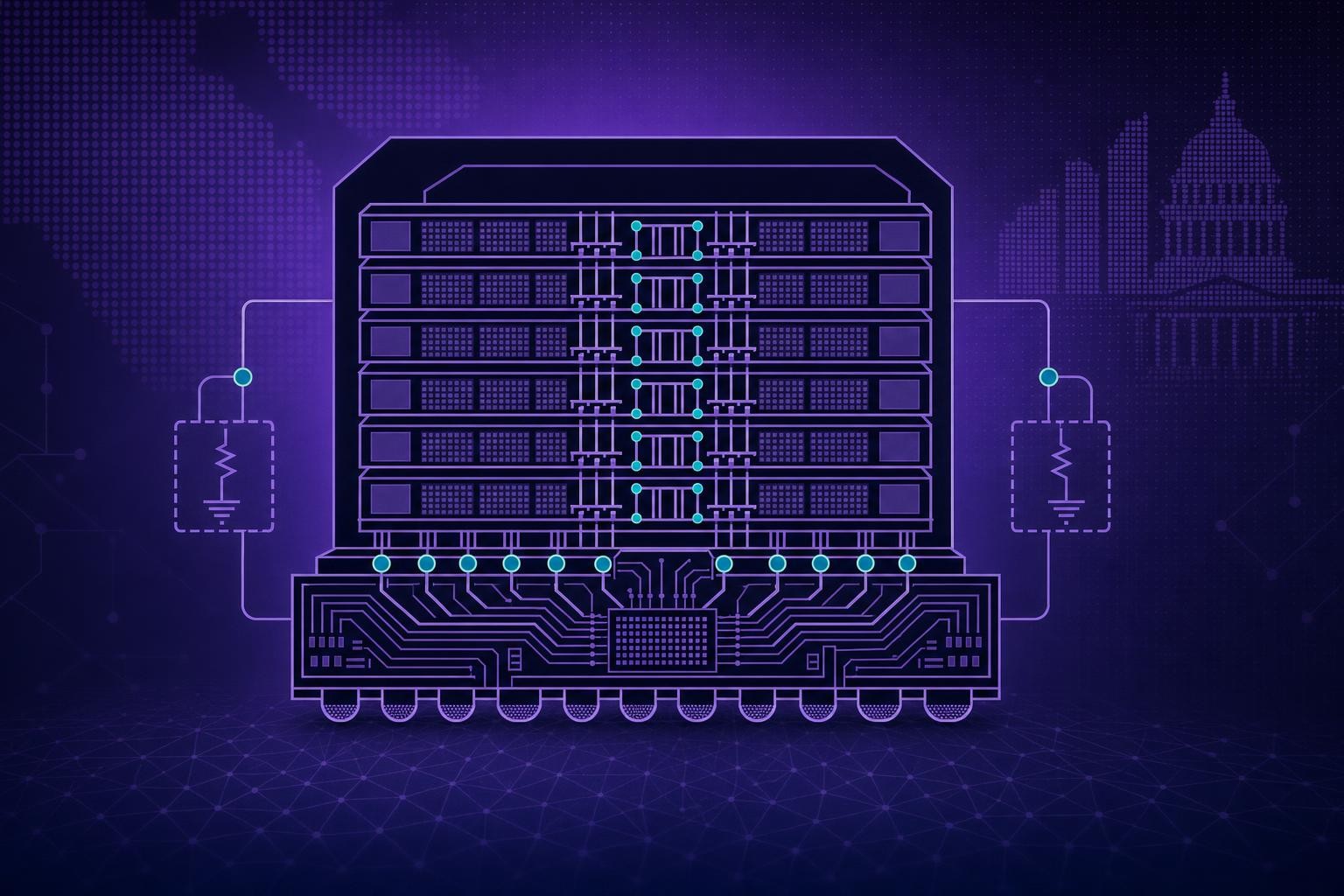 Semiconductors
ETH Zürich and NYU find JEDEC test loops underestimate HBM2 power by up to 35.4%
Researchers at ETH Zürich and NYU tested 36 real HBM2 chips and found JEDEC-specified current loops can underestimate peak power by up to 35.4%, with implications for AI accelerator thermal design.
15 Oct 2026