The Silicon Brief - 6 August 2026
Today's digest: the semiconductor market's extraordinary 2026 growth forecast, AMD's MI455X multi-die GPU, Synopsys's role in enabling it, chiplet simulation bottlenecks, and AI-augmented fab analytics.
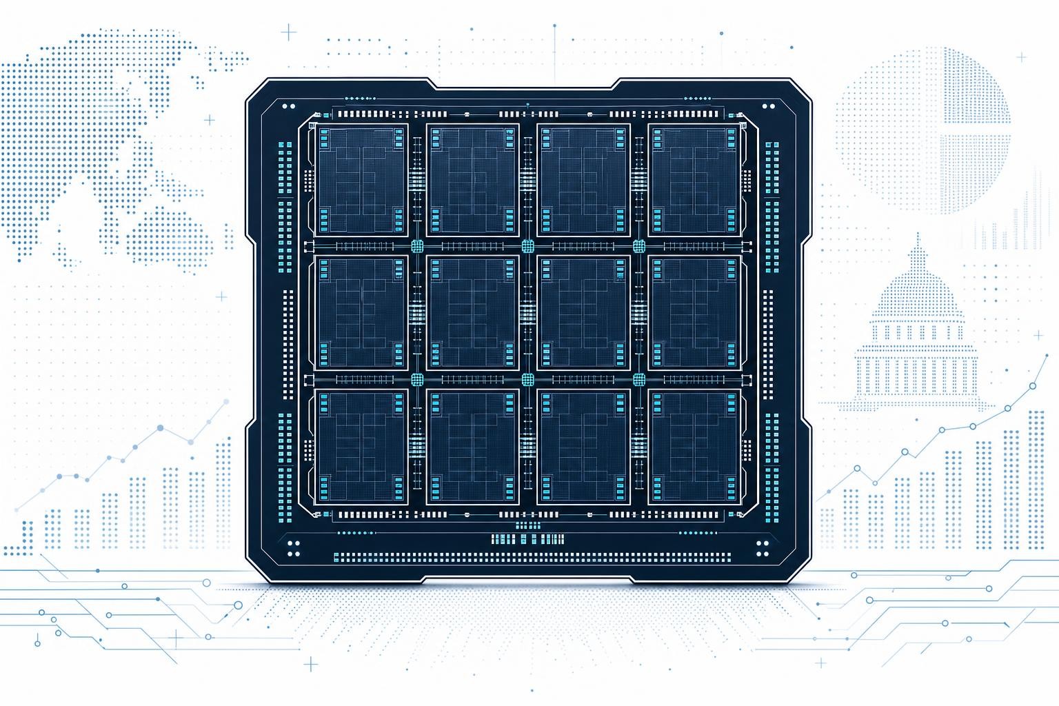
Today's edition covers the revised semiconductor market outlook for 2026, AMD's new CDNA 5 flagship accelerator and the Synopsys toolchain that helped build it, the simulation bottleneck now constraining chiplet scale-up, and the case for AI-augmented analytics inside the fab.
The McClean Report's June 2026 update raises its full-year semiconductor forecast to approximately $1.7 trillion, a 98.3% year-on-year gain, with the market projected to exceed $2.2 trillion in 2027 - a revision that reflects structural, not cyclical, demand[2]. The total memory market alone is forecast to grow 298% in 2026, reaching $916.4 billion, driven overwhelmingly by price rather than unit volume, with memory shipments expected to rise only 8%[2]. For procurement and capacity-planning teams, the implication is that supply constraints on advanced logic and HBM will persist well into next year.
AMD's Instinct MI455X, unveiled at the company's Advancing AI 2026 event, is a CDNA 5 rack-scale GPU built from twelve chiplets across TSMC N2 and N3P process nodes and packaged using CoWoS-L with 3D hybrid bonding - the first AMD accelerator designed explicitly for rack-scale deployment. The package integrates 320 billion transistors, 70% more than the MI355X, alongside 432 GB of HBM4 memory delivering 23.3 TB/s of bandwidth. Volume deployments through the 72-GPU Helios rackscale solution are expected in the second half of 2026.
Synopsys disclosed on 4 August 2026 that its multi-die EDA suite was central to the MI455X design flow, with co-simulation methodologies used to improve design quality and validate silicon readiness before tape-out[3]. The collaboration produced what AMD and Synopsys describe as a unified, automated environment from concept through advanced packaging - a template the industry will watch closely as multi-die complexity continues to grow[3].
Simulation speed, not toolchain availability, has emerged as the primary bottleneck holding chiplet programmes back, according to analysis published on 4 August 2026 - the computational cost of multi-physics co-simulation across 2.5D and 3D stacks is now the binding constraint for design teams trying to scale[1]. IDTechEx confirms chiplets are playing a crucial role across data centers, AI infrastructure, telecom, and automotive, helping overcome scaling limits, improve yields, and lower costs[1]. The practical consequence is longer verification cycles even where the underlying tooling is adequate.
EE Times published analysis on 5 August 2026 arguing that fragmented "islands of optimization" inside fabs - where etch, track, and lithography tools each run siloed native software - are the primary obstacle to detecting yield excursions in real time[4]. Leading-edge foundry capacity is reported to be pre-booked through 2028, in some cases for fabs not yet built[4], making throughput protection through AI-augmented data analytics an urgent operational priority rather than a roadmap item.
Written by Electronics Insider's automated desk from the sources above and published automatically. How we work.
Related
 Semiconductors
Token spend is becoming a line item in EDA project budgets, DAC roundtable finds
A closed-door DAC 2026 roundtable with Cadence, Synopsys, Siemens EDA, Keysight, and ChipAgents found token cost has moved from an afterthought to a formal budget concern in chip design projects.
10 Sept 2026 Design & EDA
Cadence's Amol Borkar explains why AI voice at the edge demands a rethink of SoC architecture, not just faster processors
Semiconductor Engineering's interview with Cadence's Tensilica DSP lead lays out why NLP is reshaping audio SoC design - and why raw clock speed is the wrong lever to pull.
10 Sept 2026 Design & EDA
French gendarmerie researchers show voltage glitching bypasses eMMC password locks on 3 of 10 commercial parts, with measurable evidence alteration
A paper from France's Institut de Recherche Criminelle quantifies both the success rate and the data-integrity cost of fault-assisted eMMC access in forensic investigations.
10 Sept 2026