The Silicon Brief - 9 September 2026
Today: Samsung maps a three-phase HBM roadmap toward zHBM compute-in-memory, SIA July sales hit $146.8 B for a 17th straight monthly record, SK hynix pushes hybrid bonding to HBM5, Micron flags a widening memory wall, and Huawei's FLINT paper proposes flash as an LLM inference tier.

Today's edition covers Samsung's three-phase plan to turn the HBM base die into a compute element, a fresh SIA sales record that puts the industry ahead of its best-ever full year after just seven months, SK hynix's confirmation that hybrid bonding will not arrive until HBM5, Micron's warning that the memory wall is widening with every generation, and a new academic paper proposing high-bandwidth flash as a scalable capacity tier for LLM inference.
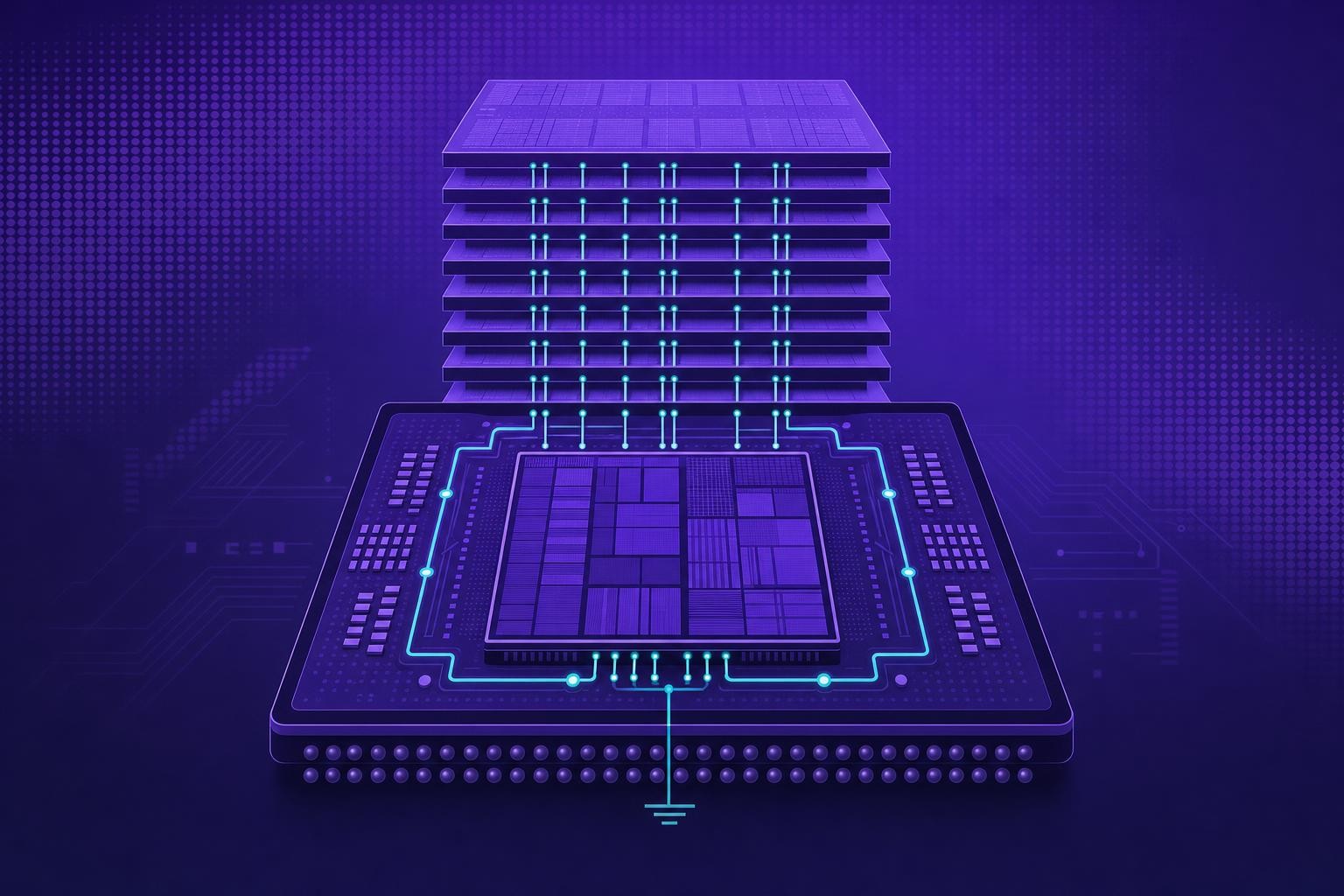
Samsung unveiled a three-phase roadmap at Hot Chips 2026 to transform the HBM base die from a passive interface into an SoC-like compute element, culminating in zHBM, which stacks DRAM directly on top of the processor and eliminates the conventional 2.5D interposer. [1] Starting with HBM4, Samsung moved the base die to a 4 nm logic process, primarily to reduce power draw and minimize die area, which left substantial unused silicon that the company now proposes to fill with memory controllers, RAS sensors, processing elements, and eventually selected accelerator functions. Phase 1 offloads the memory controller from the GPU onto the B-die, freeing GPU area for compute; Phase 2 adds telemetry and direct memory-extension logic; Phase 3 - zHBM - bonds DRAM vertically onto the processor, requiring advanced wafer-on-wafer and hybrid copper bonding. Samsung did not give a firm timeline for the later phases, but the argument matters to any system architect planning around HBM5 and beyond: the base die is becoming a co-processor, and that changes where logic is partitioned across an AI accelerator package.[1]
SK hynix confirmed at Hot Chips 2026 that hybrid bonding will not be ready for HBM4E and is now targeted at HBM5 at the earliest, extending the company's mass-reflow molded-underfill process through Nvidia's Rubin platform. The binding constraint is physical: HBM stacks are capped at a total height of 775 microns - the standard thickness of a 300 mm logic wafer - so every additional DRAM layer requires thinner dies and narrower gaps, and hybrid bonding's room-temperature pick-and-place followed by a high-temperature anneal has not yet met yield requirements at that geometry. The slip matters because hybrid bonding is the primary route to the tighter pitch needed for 20-high stacks and beyond; without it, thermal resistance and die-thinning yield remain the binding constraints on HBM capacity scaling.
Micron warned at Hot Chips 2026 that the gap between compute performance scaling and HBM bandwidth is widening, not closing, with compute advancing roughly three times every two years against HBM bandwidth growth of under two times. HBM already consumes approximately three times more silicon per bit than DDR5, and each generation of wider host interfaces - HBM4 doubles to 2,048 I/Os - enlarges the die further, compounding the wafer-capacity penalty. The practical consequence is that the DRAM shortage AI demand has created is structural rather than cyclical: more HBM per accelerator means fewer conventional DRAM wafers, and the silicon ratio widens with every node.
The SIA reported on 4 September 2026 that global semiconductor sales reached $146.8 billion in July, a 135.1% year-on-year increase and the seventeenth consecutive month of sequential growth, with cumulative 2026 sales already exceeding the industry's previous highest full-year total. July's $146.8 billion figure was 6.4% above June's $137.9 billion and 135.1% higher than the $62.5 billion recorded in July 2025, and every regional market tracked by SIA grew both year-on-year and month-on-month. The milestone - a full-year record crossed in seven months - reflects the scale of AI infrastructure spending rather than broad-based demand recovery; automotive, consumer, and smartphone chips remain in slower-growth territory while memory and advanced logic for data centres drive the headline numbers.
Huawei, ETH Zürich, and HUST published FLINT, a hardware-software substrate that uses high-bandwidth flash as a capacity tier alongside HBM for LLM inference, addressing the memory-capacity constraint that limits deployable model size on single accelerators. [2] FLINT introduces a burst-buffer controller, a phantom-plane refresh mechanism, and a read-only flash translation layer to sustain high HBF bandwidth without exposing NAND management tasks to the inference critical path, targeting the class of inference systems where HBM alone cannot hold the full weight set of a large model. The paper is one of several in Semiconductor Engineering's 8 September technical roundup pointing toward heterogeneous memory hierarchies - HBM for bandwidth, flash for capacity - as the near-term answer to the memory wall, before processing-in-memory architectures mature.[2]
Written by Electronics Insider's automated desk from the sources above and published automatically. How we work.
Related
 Design & EDA
ETH Zürich and NYU show JEDEC test loops miss worst-case HBM2 power by 23.6%
Researchers at ETH Zürich and NYU tested 36 real HBM2 chips and found JEDEC measurement loops understate peak power by 23.6%, with read ops and data-bus toggling as the main drivers.
15 Oct 2026 Design & EDA
FlowAccel's Joel Jorgensen argues chip teams must design their workflows before AI can help them hit tape-out
Joel Jorgensen of FlowAccel argues that AI tools alone won't save a tape-out schedule - teams must first design the cross-team workflows that let those tools compound into real gains.
15 Oct 2026 Semiconductors
ETH Zürich and NYU find JEDEC test loops underestimate HBM2 power by up to 35.4%
Researchers at ETH Zürich and NYU tested 36 real HBM2 chips and found JEDEC-specified current loops can underestimate peak power by up to 35.4%, with implications for AI accelerator thermal design.
15 Oct 2026