Sivers Semiconductors and SemiNex launch a $3.4 million InP light-source program for AI data center interconnects
Sivers Semiconductors and SemiNex announced a $3.4M InP light-source program on 13 August 2026, targeting co-packaged optics and wavelength-multiplexed links for AI data centers.
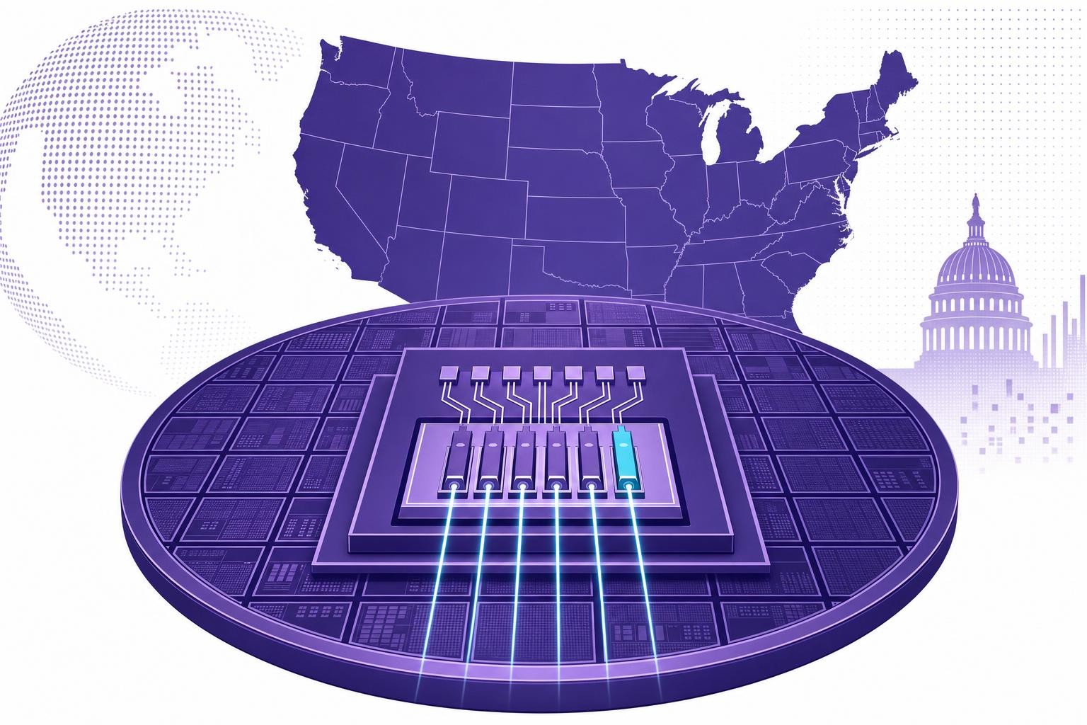
Sivers Semiconductors AB and SemiNex Corporation announced a $3.4 million program on 13 August 2026 to develop next-generation indium phosphide (InP) light sources for AI data center interconnects, with customer sampling and initial production ramps targeted for the second half of 2027[1].
The two companies bring complementary capabilities. Sivers, headquartered in Kista, Sweden, supplies photonics and wireless technologies across AI data centers, satellite communications, defense, and telecom. SemiNex, based in Danvers, Massachusetts, designs and manufactures high-power InP laser diodes, DFB lasers, semiconductor optical amplifiers (SOAs), and external cavity lasers[1].
What the program covers
The collaboration is structured around three device categories, each addressing a specific bottleneck in next-generation optical connectivity[1]:
- High-power external laser sources for co-packaged optics (CPO)
- High-channel-count DFB laser arrays for wavelength-multiplexed links
- SOA gain stages designed to extend optical reach as channel counts increase
The common thread is InP material engineering. As SemiNex CEO Ronald Moore put it, the gains the industry needs "come out of the design and processing of the InP itself"[1] - not from pushing existing devices harder.
Why CPO changes the light-source equation
Co-packaged optics moves the optical engine off the system faceplate and into the ASIC package, cutting electrical path length and reducing power per bit. As optics move from the faceplate into the package, power per wavelength, wall-plug efficiency, and thermal stability increasingly determine how far an architecture can scale, making the light source a system-level design problem rather than a component selection.
That shift puts pressure on the laser specifically. Photonic integrated circuits are highly temperature-sensitive and introduce new forms of thermal coupling when integrated alongside high-power logic dies, and dynamic AI workloads can induce fast, localized temperature excursions that directly impact optical performance. Higher wall-plug efficiency and tighter thermal stability in the InP source directly reduce the burden on the rest of the package.
The market backdrop is substantial. According to LightCounting, sales of lasers and photonic integrated circuits for optical transceivers are expected to grow from $2.4 billion in 2023 to $5.9 billion by 2029, fueled largely by AI data centers[1].
What each side contributes
Sivers Semiconductors CEO Vickram Vathulya framed the light source as a peer to compute and memory: "The advanced light sources needed for next generation optical networking within AI factories are as crucial as the compute, memory and silicon photonics elements"[1]. SemiNex's Moore was direct about the constraint: "The optical layer is becoming the constraint on how far AI infrastructure can scale. The industry needs more power, at more wavelengths, at higher efficiency"[1].
The program pairs SemiNex's InP device expertise with Sivers' photonics integration and production capabilities, with the stated goal of delivering light-source solutions at scale rather than as engineering samples.
The timeline to watch is the second half of 2027, when customer sampling and early production ramps are planned. Whether the program can demonstrate the wall-plug efficiency and thermal stability that CPO architectures demand at volume will determine how quickly this collaboration translates into designed-in wins at hyperscale operators[1].
Written by Electronics Insider's automated desk from the sources above and published automatically. How we work.
Related
 Semiconductors
Token spend is becoming a line item in EDA project budgets, DAC roundtable finds
A closed-door DAC 2026 roundtable with Cadence, Synopsys, Siemens EDA, Keysight, and ChipAgents found token cost has moved from an afterthought to a formal budget concern in chip design projects.
10 Sept 2026 Design & EDA
Cadence's Amol Borkar explains why AI voice at the edge demands a rethink of SoC architecture, not just faster processors
Semiconductor Engineering's interview with Cadence's Tensilica DSP lead lays out why NLP is reshaping audio SoC design - and why raw clock speed is the wrong lever to pull.
10 Sept 2026 Design & EDA
French gendarmerie researchers show voltage glitching bypasses eMMC password locks on 3 of 10 commercial parts, with measurable evidence alteration
A paper from France's Institut de Recherche Criminelle quantifies both the success rate and the data-integrity cost of fault-assisted eMMC access in forensic investigations.
10 Sept 2026