TSMC's CoWoS-S silicon interposer reaches ~2500 mm² in its fifth generation to meet AI accelerator bandwidth demands
TSMC's fifth-generation CoWoS-S uses a mask-stitched silicon interposer at ~2500 mm² to co-integrate logic dies and HBM stacks for AI accelerators - and the roadmap goes further still.
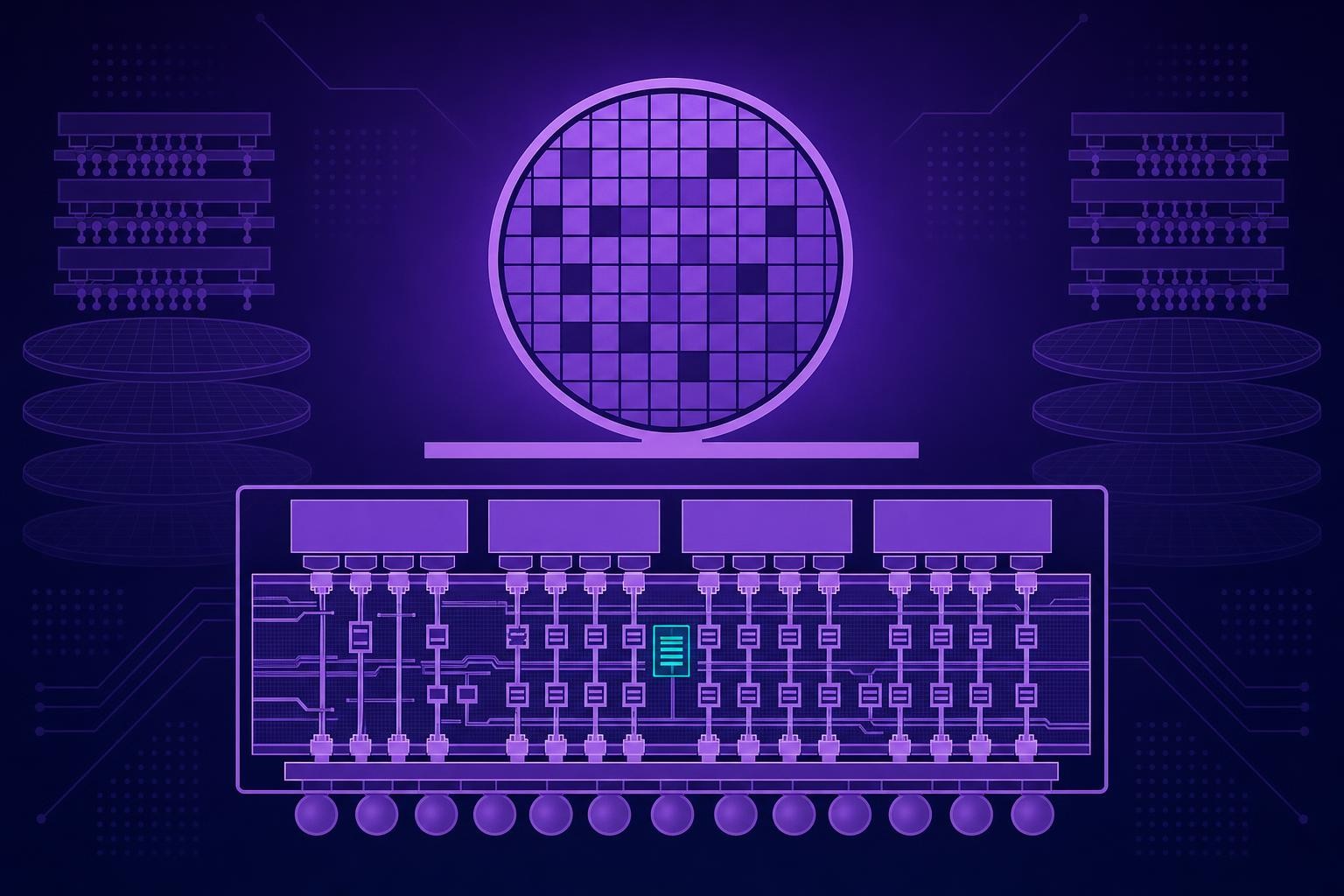
A SemiWiki analysis published in August 2026 examines why TSMC's CoWoS-S - Chip-on-Wafer-on-Substrate with a silicon interposer - has become the structural foundation of modern AI accelerators[1]. The central problem it solves is architectural: compute capability is scaling faster than conventional packages can supply data, power, and connectivity[1]. The fifth-generation variant, CoWoS-S5, addresses this by expanding the silicon interposer to ~2500 mm² through a novel mask-stitching approach, up from ~830 mm² in the first generation.
What CoWoS-S actually does
CoWoS-S is a 2.5D multi-chip integration technology. A logic die - typically a GPU or AI accelerator - and several stacks of High Bandwidth Memory (HBM) are placed side by side on a passive silicon interposer. The interposer is threaded with through-silicon vias (TSVs) that route signals vertically down to an organic substrate, enabling memory bandwidth in the terabytes-per-second range that standard PCB traces cannot approach.
The silicon interposer does more than route signals. TSMC's integrated capacitor (iCAP) technology, embedded in the interposer as deep trench capacitors with a standard cell of 40 µm by 40 µm, achieves a capacitance density of up to 340 nF/mm² - roughly 20× the density of conventional metal-insulator-metal capacitors. TSMC reports that iCAP reduces power-delivery-network impedance to 0.05× and voltage droop to 0.45× compared to equivalent CoWoS designs without it.
How the interposer has grown
The interposer size has expanded steadily to accommodate more active silicon per package:
- Generation 1: ~830 mm² (one full reticle)
- Generation 3: ~1700 mm² (two reticles)
- CoWoS-S5: ~2500 mm² (three reticles, mask-stitched)
- CoWoS-L roadmap target (2027): 9.5-reticle interposer supporting 12 HBM5 stacks on a 120 mm × 150 mm substrate
CoWoS has been in volume production since 2012, but demand accelerated sharply after generative AI emerged in late 2022. TSMC's own roadmap, presented at its North America Technology Symposium in May 2026, projects interposer sizes reaching over 14 reticles by 2029, supporting up to 24 HBM stacks - a configuration TSMC claims will deliver 48× the compute transistor count and 34× the memory bandwidth of a high-end data-center system-in-package from 2024.
Why CoWoS-S rather than CoWoS-L
TSMC offers three CoWoS variants. CoWoS-S uses a full silicon interposer and is recommended for packages up to 3.3× reticle size. CoWoS-L uses hybrid RDL and silicon bridges for larger packages - it is the format used in NVIDIA's Blackwell GPUs. CoWoS-R uses an organic RDL interposer for cost-sensitive designs. Virtually all flagship AI accelerators from NVIDIA, AMD, and Broadcom rely on one of these two leading variants.
The manufacturing complexity of CoWoS-S5 is significant. Yield for mature CoWoS-S runs is estimated at 60-80%, and a single defect can destroy a package worth more than $50,000. Setting up new packaging capacity requires specialized equipment - ultra-precise pick-and-place machines and thermal compression bonders - with lead times of 12 to 18 months, which is why packaging, not wafer fabrication, is now the binding constraint on AI accelerator output.
The next milestone to watch is CoPoS - a hybrid approach that uses fine-pitch silicon only where needed and organic redistribution layers elsewhere - which TSMC has indicated will enter pilot production in 2026 with a volume ramp targeted around 2029. Whether CoPoS can relieve interposer cost pressure while preserving the signal-integrity advantages of CoWoS-S will determine how the packaging roadmap evolves beyond the current generation.
Written by Electronics Insider's automated desk from the sources above and published automatically. How we work.
Related
 Semiconductors
Token spend is becoming a line item in EDA project budgets, DAC roundtable finds
A closed-door DAC 2026 roundtable with Cadence, Synopsys, Siemens EDA, Keysight, and ChipAgents found token cost has moved from an afterthought to a formal budget concern in chip design projects.
10 Sept 2026 Design & EDA
Cadence's Amol Borkar explains why AI voice at the edge demands a rethink of SoC architecture, not just faster processors
Semiconductor Engineering's interview with Cadence's Tensilica DSP lead lays out why NLP is reshaping audio SoC design - and why raw clock speed is the wrong lever to pull.
10 Sept 2026 Design & EDA
French gendarmerie researchers show voltage glitching bypasses eMMC password locks on 3 of 10 commercial parts, with measurable evidence alteration
A paper from France's Institut de Recherche Criminelle quantifies both the success rate and the data-integrity cost of fault-assisted eMMC access in forensic investigations.
10 Sept 2026