ZEISS launches Crossbeam 750 FIB-SEM with continuous SEM imaging during milling for leading-edge failure analysis
ZEISS unveiled the Crossbeam 750 FIB-SEM on 31 March 2026, combining Gemini 4 optics with HDR Mill + SEM to deliver uninterrupted, real-time imaging during low-kV FIB finishing for advanced-node TEM lamella prep.
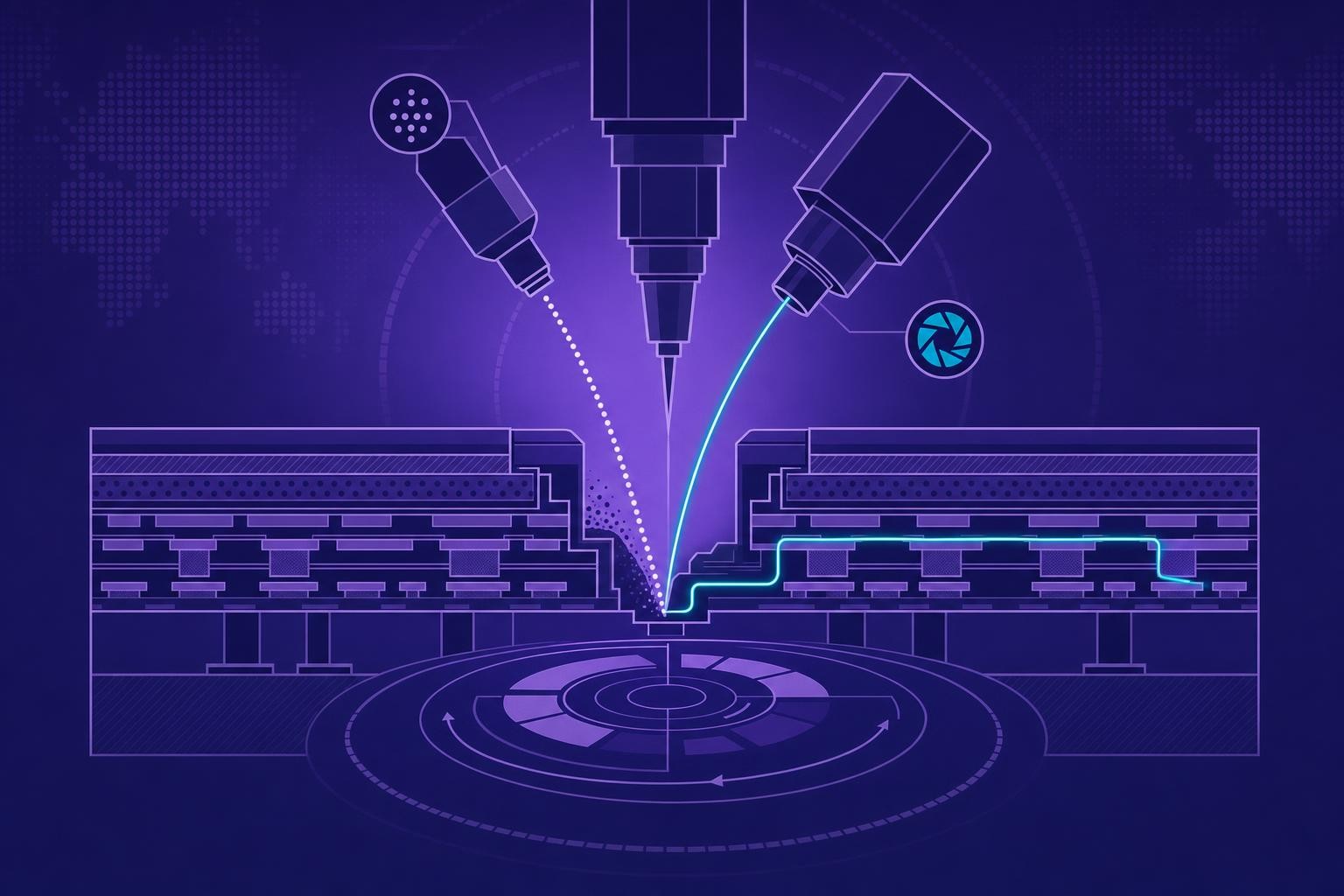
ZEISS unveiled the Crossbeam 750 FIB-SEM on 31 March 2026, introducing a "see while you mill" capability that keeps a live, high-resolution SEM view active at every stage of focused ion beam processing - from rapid bulk removal down to fine polishing at 0.5 kV[1]. The instrument targets semiconductor failure analysis teams working on leading-node logic and memory devices where conventional stop-mill-image cycles introduce damage, misalignment, and rework.
The problem with stopping to look
Traditional FIB-SEM workflows require the operator to pause milling in order to acquire an SEM image and check progress. This intermittent imaging can lead to inaccuracies in endpoint detection and increased rework. The issue sharpens at advanced nodes: as semiconductor device architectures shrink and complexity increases - from FinFET to gate-all-around (GAA), complementary FET (CFET), and emerging 2D materials - precise, real-time control during FIB processing has become critical.
A further complication is that low-kV finishing, which is necessary to minimise the amorphised damage layer left by high-energy ions, has historically degraded probe-forming performance. A high-energy focused ion beam (e.g., 30 kV) produces a substantial damage layer in the final lamella, yet FIB resolution and probe characteristics are degraded at low-kV because chromatic aberrations substantially reduce probe-forming performance. The result has been a difficult trade-off between surface quality and positional accuracy.
What Crossbeam 750 changes
The Crossbeam 750 addresses both constraints through three integrated hardware advances[1]:
- Gemini 4 field-free objective lens - delivers background-free, real-time endpointing and sub-nanometer precision for TEM lamellae across the full range of landing energies
- Double deflector and next-generation scan generator - maintains image stability and alignment during simultaneous milling and imaging
- HDR Mill + SEM mode - an interwoven SEM/FIB scanning sequence that suppresses FIB-generated background, enabling clean visual feedback even while nudging the milling pattern live
With HDR Mill + SEM, buried features remain clearly visible throughout thinning, supporting confident endpoint control and repeatable sub-20 nm lamella preparation for advanced semiconductor structures such as fins, vias, and gate stacks. Low-energy FIB finishing minimises amorphisation and preserves fine details.
"ZEISS Crossbeam 750 was designed around one core principle: our customers should not have to stop milling to see where in their sample they are working," said Dr. Thomas Rodgers, senior director of market strategy, head of business sector electronics, ZEISS Microscopy. "Our new HDR Mill + SEM capability maintains a clear, high-resolution SEM view at any FIB condition, from rapid milling with high FIB currents down to fine polishing at 0.5 kV."
Workflow impact for FA and yield teams
By eliminating the need to pause milling for imaging, the Crossbeam 750 streamlines workflows and reduces total processing time. Continuous monitoring enables more consistent results, particularly in high-throughput environments where reproducibility is critical. The ability to achieve precise endpoints on the first attempt is especially valuable in semiconductor failure analysis and process development, where deviations at the nanometer scale can affect device performance.
The system also supports atom probe tomography (APT)-ready lift-out and 3D tomography with a larger, undistorted field of view, reducing acquisition time for volume imaging workflows[1]. It is positioned as ideal for analysis of leading-node logic and memory devices as well as nanofabrication and 3D volume imaging.
ZEISS is hosting a dedicated webinar - "SEM-Guided Low-kV FIB Finishing for Leading-Edge Semiconductor Failure Analysis" - to demonstrate the HDR Mill + SEM mode live, including real-time pattern adjustment during milling[1]. The session is aimed at failure analysis engineers, yield teams, and materials scientists who need faster time-to-TEM and higher first-pass success rates. Whether the Crossbeam 750's continuous-imaging approach becomes the new baseline for advanced-node FA workflows will depend on how it performs against plasma-FIB alternatives at sub-3 nm nodes, where sample volumes and throughput demands continue to grow.
Written by Electronics Insider's automated desk from the sources above and published automatically. How we work.
Related
 Semiconductors
Token spend is becoming a line item in EDA project budgets, DAC roundtable finds
A closed-door DAC 2026 roundtable with Cadence, Synopsys, Siemens EDA, Keysight, and ChipAgents found token cost has moved from an afterthought to a formal budget concern in chip design projects.
10 Sept 2026 Design & EDA
Cadence's Amol Borkar explains why AI voice at the edge demands a rethink of SoC architecture, not just faster processors
Semiconductor Engineering's interview with Cadence's Tensilica DSP lead lays out why NLP is reshaping audio SoC design - and why raw clock speed is the wrong lever to pull.
10 Sept 2026 Design & EDA
French gendarmerie researchers show voltage glitching bypasses eMMC password locks on 3 of 10 commercial parts, with measurable evidence alteration
A paper from France's Institut de Recherche Criminelle quantifies both the success rate and the data-integrity cost of fault-assisted eMMC access in forensic investigations.
10 Sept 2026