ETH Zürich and NYU show JEDEC test loops miss worst-case HBM2 power by 23.6%
Researchers at ETH Zürich and NYU tested 36 real HBM2 chips and found JEDEC measurement loops understate peak power by 23.6%, with read ops and data-bus toggling as the main drivers.
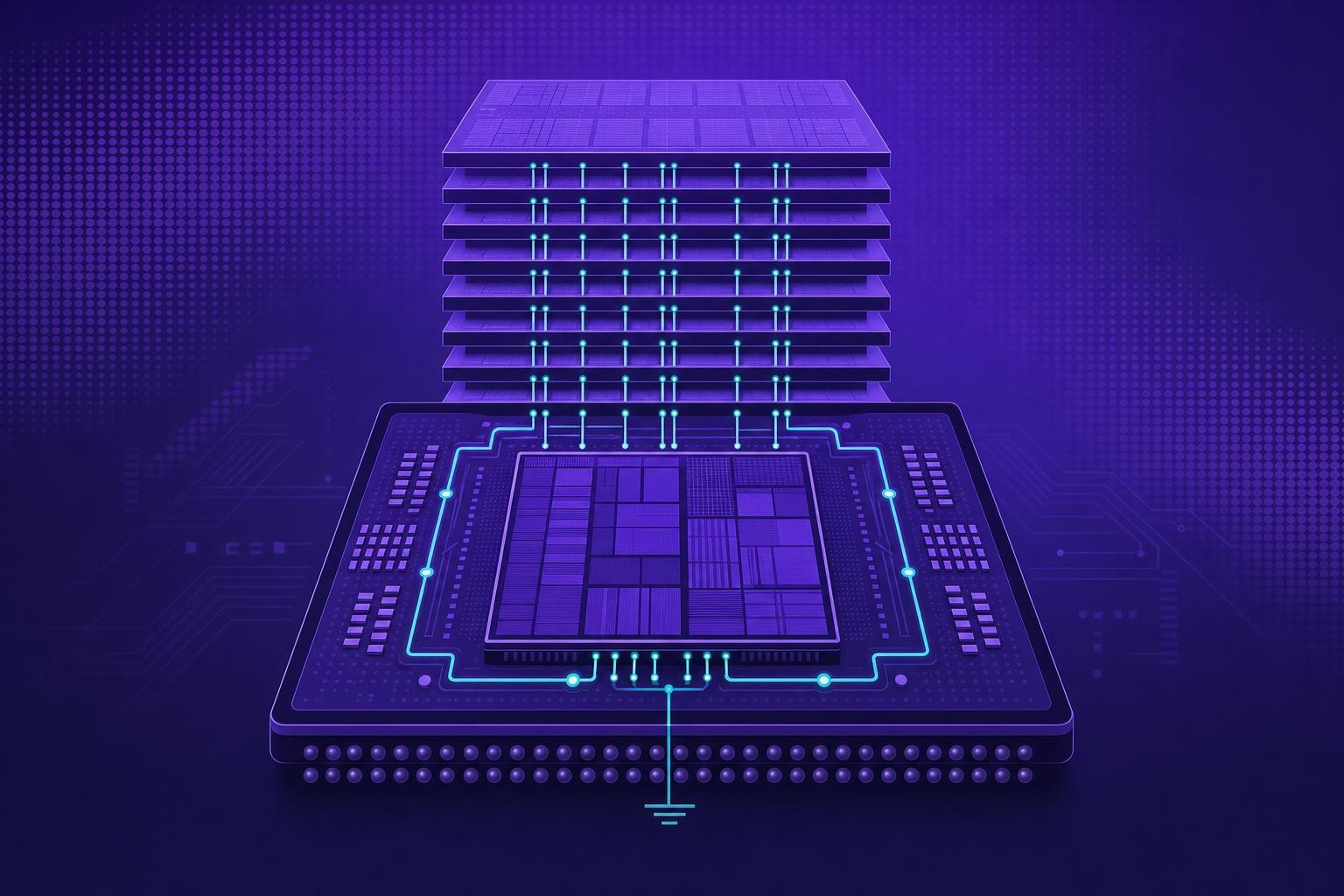
Researchers at ETH Zürich and New York University published a paper on 9 October 2026 reporting the first comprehensive experimental characterization of power consumed by real HBM2 DRAM chips[1]. Testing 36 chips across 18 AMD Alveo U55C FPGA boards, the team found that a custom access pattern they engineered draws 23.6% more power on average than the highest-power-consuming JEDEC-specified current measurement loop[1] - a gap with direct consequences for thermal budgeting in AI accelerator systems.
What the measurements revealed
The study produced 13 new findings and 6 key takeaway messages on HBM2 power behavior[1]. Three results stand out:
- Read operations consume significantly higher current than any other HBM2 operation, including writes and activates[1].
- Data-bus toggling is a major power driver: toggling all HBM2-internal bank group bus signals during a burst transfer causes 29.4% higher power consumption than keeping those signals constant[1].
- Structural variation across bank groups and banks is real and measurable - uniform power models that assign equal consumption to all exercised bank groups cannot accurately capture the actual power distribution across an HBM2 channel[1].
The team used an FPGA-based testing platform built on DRAM Bender, which can execute arbitrary low-level DRAM command sequences targeting fine-grained structures across any combination of HBM2 channels[1].
Why existing models fall short
The paper argues that standard JEDEC current measurement loops rely on fixed data patterns that do not capture the highest-power-consuming access modes[1]. State-of-the-art HBM power models carry prediction errors between 20% and 42% - for example, DRAMSim3 shows 21.6% mean absolute percentage error on the workloads the team evaluated. A model that describes all data-bus toggling activity with a single parameter yields 11.4% error in read energy per bit even after calibration to the team's own measurements.
Relying solely on JEDEC- or vendor-specified test loops to bound HBM power could cause system failures or thermal throttling under real-world AI and machine-learning workloads[1].
A new model and its accuracy
To address the gap, the researchers developed a new HBM power model grounded in their empirical characterization. The model predicts power across 36 HBM2 chips and diverse workloads - including a real Llama 3.1-8B decode trace - with 7.6 to 8.1% mean absolute percentage error, substantially below the 20-42% range of prior art. The team also validated the model against measured HBM3E memory power on an NVIDIA H200 GPU, extending its relevance beyond the HBM2 generation tested directly.
Source code, all characterization data, and workload traces are available in the CMU-SAFARI/HBM-Power repository on GitHub, and the full paper is on arXiv at arXiv:2610.14244.
As HBM4 and HBM4E enter production and stack heights continue to rise, the question of whether JEDEC test loops keep pace with real workload power envelopes will matter more, not less, to system designers specifying power delivery and thermal management for next-generation AI accelerators.
Written by Electronics Insider's automated desk from the sources above and published automatically. How we work.
Related
 Design & EDA
FlowAccel's Joel Jorgensen argues chip teams must design their workflows before AI can help them hit tape-out
Joel Jorgensen of FlowAccel argues that AI tools alone won't save a tape-out schedule - teams must first design the cross-team workflows that let those tools compound into real gains.
15 Oct 2026 Semiconductors
ETH Zürich and NYU find JEDEC test loops underestimate HBM2 power by up to 35.4%
Researchers at ETH Zürich and NYU tested 36 real HBM2 chips and found JEDEC-specified current loops can underestimate peak power by up to 35.4%, with implications for AI accelerator thermal design.
15 Oct 2026 Semiconductors
Sandia and Luxembourg researchers map the exact leakage route in gate-all-around transistors
Researchers at Sandia and Luxembourg's LIST used quantum-transport simulations to spatially resolve gate-drain tunneling in GAAFETs, pinpointing where leakage current flows at the device level.
15 Oct 2026